
Beijing’s efforts to counteract U.S. sanctions that have hindered China’s ability to produce cutting-edge chips are highlighted by Huawei Technologies’ announcement on Monday that it will produce industry-leading semiconductors using a new technology in five years.
At a semiconductor symposium in Shanghai, Huawei claimed that by 2031, its high-end processors would have transistor densities comparable to 1.4-nanometer processes, but it did not offer any independent performance statistics.
The goal is important because, by the end of the decade, 1.4 nm is predicted to be near the worldwide boundary for advanced chipmaking, whereas China’s most advanced proven chipmaking capabilities are widely recognized at about 7 nm.
Since Washington has limited China’s access to cutting-edge lithography equipment and other crucial semiconductor technologies, it is generally believed that China is unlikely to achieve that level through traditional production alone.
The largest manufacturer of the most cutting-edge chips in the world is Taiwan’s TSMC. It presently employs a 2-nm manufacturing technique and intends to implement a 1.4-nm process for mass production in 2028.
“TAU SCALING LAW”
Moore’s Law, which states that the industry can no longer rely on reducing transistors for computing advancements since they are now so small that their dimensions are measured in only a few atoms, was revealed by Huawei on Monday, along with a new premise for upgrading semiconductors.
According to Huawei, the idea known as the Tau Scaling Law instead concentrates on reducing the time it takes for signals and data to pass through semiconductors and computer systems.
Although the global chip industry is spending more on post-Moore’s Law solutions, such as chiplets and sophisticated packaging, the quest has become particularly pressing for China.
Chinese businesses’ access to the most sophisticated chipmaking equipment, especially that required to produce chips at cutting-edge process nodes, has been hampered by U.S. export regulations.
“What Huawei is proposing is a shift from traditional node-driven scaling to system-level efficiency scaling,” stated He Hui, director of semiconductor research at Omdia.
As a result, Beijing’s goal of creating a world-leading and self-sufficient semiconductor industry has made alternative routes to higher performance crucial.
The business is concentrating on shortening connections, reducing latency, and enhancing data mobility inside the device rather than relying just on fewer transistors.
This is a reliable method of extracting greater performance when cutting-edge lithography is limited.”
AI BOOM INCREASES STAKES
Because frontier technologies are becoming a crucial component of China’s future economic growth and geopolitical might, the stakes for Huawei’s chip innovations are doubled.
Chinese AI models, such as DeepSeek’s most recent flagship model V4, which was unveiled last month, rely heavily on Huawei’s Ascend chip family.
Huawei said that its Kirin smartphone chips, which are slated for release later this year, will be the first to employ a Tau Scaling architecture known as LogicFolding.
The company claimed that this would save internal chip wiring and significantly boost performance.
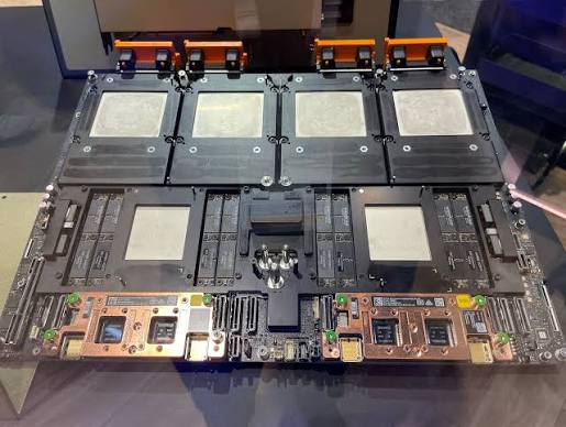
By 2030, the company plans to apply LogicFolding to Ascend chips as well as huge AI clusters that run data centers and consist of hundreds or thousands of chips.
It further stated that over the last six years, its chip division has created and mass-produced 381 semiconductors based on the Tau Scaling Law for usage in sectors including AI computers and cellphones.
A DOMESTIC NVIDIA SUBSTITUTE
In 2019, Huawei was placed on a U.S. trade blacklist, which limited its ability to rely on international contract chipmakers and cut it off from several U.S.-origin technologies, such as chips and software.
After the limitations were put in place, Huawei went into what it called “extreme survival mode.”
A key component of Huawei’s survival strategy was a covert backup chip project headed by He Tingbo, president of the company’s semiconductor division and director of its Science Committee.
With the release of its 5G-capable Mate 60 series smartphones in 2023, the business made an unexpected comeback.
These devices were powered by a system-on-a-chip made by Semiconductor Manufacturing International Corp (SMIC), China’s largest contract chipmaker using 7-nm technology.
Following Huawei’s unveiling of its LogicFolding architecture, SMIC shares increased 7.6% on Monday. Additionally, SMIC recently made investments in post-Moore’s Law pathways, establishing an advanced packaging research lab in Shanghai in January.
China’s chip market is rising.
This year, demand for Ascend chips has increased in China as local tech companies look for alternatives to Nvidia, a U.S. company whose most cutting-edge AI processors are prohibited from being sold to China.
Earlier this month, Nvidia CEO Jensen Huang declared that the business had “largely conceded” to Huawei in the Chinese AI chip market.
Analysts note that although China has made improvements, it still lags behind world leaders in the most sophisticated industrial technology.
Cost, power, heat, and system integration continue to be significant obstacles, particularly for Cloud AI servers, according to Brady Wang, associate director at Counterpoint Research.
“In the short term, China may narrow the gap with global leaders, but a technology gap with the most advanced nodes will remain,” he said.
The chip head of Huawei He admitted that there are still significant obstacles to its most recent strategy, such as the requirement for new chip-design tools appropriate for Tau Scaling and the difficulty of avoiding overheating in anything from mobile chips to massive AI data centers.
Considering all the different limitations, we’ve come up with a few decent options. “I am confident that our mobile and AI computing solutions will be competitive in the next ten years,” he stated.